Surface Mount Technology and Devices – Past and Present
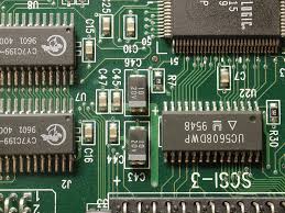
There is a strong likelihood of at least one PCB on a circuit design inside any product today. Electronic components enable all classes of end-products, providing everything from power conversion to process control. The need for densely populated PCBs is apparent for small and portable devices, but the trend for smaller outlines and lower profiles now extends to all products. Size matters, of course, but it is also a matter of mass production and lowering the average selling price through high volumes. To be competitive, most active and passive electronic components have to be offered in a surface-mount package if at all possible.
The underlying technology has been around for decades. Still, it continues to evolve, aligned with the semiconductor industry’s insatiable thirst for higher functional density – but the benefits associated with surface-mount technology (SMT) extend to all applications areas. These can be summarized, as shown below.
Cost
The cost of an integrated device is linked to its size in terms of the materials needed to produce it. This is one reason why the die inside integrated devices gets cheaper as it shrinks in size, thanks to Moore’s Law and developments in the fabrication process.
However, it is also important to appreciate that the cost of manufacturing the PCB is also reduced when using surface-mount devices (SMDs) instead of through-hole components. This is because the automated production assembly is more efficient, quicker, and less prone to error. Manufacturing errors are extremely expensive, in relative terms. It may not be cost-effective to rework a PCB with misplaced through-hole components, improper solder connections, and other issues induced by human error. SMD components are placed atop the board with pick and place machinery, and the solder flows on one side only, which is more easily controlled and more efficient. SMD assembly is automated, which reduces the amount of human interaction and labor required and, therefore, the cost of production.
Space
Of course, SMDs are smaller than their through-hole counterparts. This is essential because the pitch between the SMD pads is much smaller than the pitch between pins on a through-hole component. The larger pitch of a through-hole pin is needed to support the hole diameter and the pad around the hole for the solder to bond with.
A smaller pad pitch translates to higher PCB density and, in turn, a smaller PCB. The cost of PCB fabrication is typically based on the physical dimensions of the PCB’s footprint, so a smaller footprint also means a lower PCB cost.
Quality
While all components are produced to high-quality standards, there is less chance for manufacturing errors when using surface-mount components. This means the overall level of quality for the end-product goes up.
Limitations
The clear advantages of SMT would suggest it should be used exclusively. However, there are good reasons why through-hole packaging is still important. Foremost, SMT is mainly restricted to low power active (semiconductor) devices and is less suitable for high-voltage discrete power semiconductors, such as MOSFETs or IGBTs (although they are available). Similarly, high-power passive components are not suitable for SMD packaging. These types of components are likely to use leads for mounting them on a PCB, so they will always be associated with through-hole technology.
The Evolution of Surface-Mount Packaging
SMT is a constantly developing area, where specialists in the final assembly and test of electronic components are always looking at new possibilities.
Integrated Circuits
Integrated circuits are the primary driver in SMT. As logic transistor dimensions continue to shrink and their density increase, new packages are developed to take advantage of the higher level of integration. Surface-mount ICs are predominantly packaged in leaded or leadless outlines. Leaded packages take the form of the J-lead (which curves away from the body of the package) and the Gull Wing (which curves under the package). Leadless chips feature arrays of balls or flush pads. The contacts on these packages are often arranged in a grid, which means a package can have many more pins than a leaded chip, which only has four edges available to it for contact placement.
Actives
The use of discrete transistors is still widespread and these, too, are available in surface-mount outlines. The Small Outline Transistor, or SOT package series, is used for small-signal transistors but can also accommodate a reasonable amount of power for switching transistors.
Passives
Surface-mounted two-terminal passive components are believed to be the most prolific, and it is easy to see why. For every single integrated circuit, there are perhaps ten or more passive components supporting it. With dimensions that measure as little as 0.125 mm by 0.25 mm (008004), they are little more than the size of a dust mote. It is hard to believe they could be made any smaller. These types of devices are also used in modules that, themselves, may only measure a few mm on each side.
Connectors
The benefits of SMT relate to automated manufacturing. These benefits are also present for components whose outline needs to comply with a fixed shape and size. Here, the attraction is not just in reducing the overall size of the component (although that is also possible with connectors) but also in improving the overall manufacturing process. This is one of the motivations behind developing surface-mount PCB edge connectors.
Trends in Surface-Mount Technology
Advancements in automated manufacturing and assembly have enabled new possibilities in the design and construction of electronic components. Surface mount technology is the perfect companion to these advances, enabling engineering teams to innovate at a greater scale.
Surface- Mount transformers
The IoT has generated many new applications, many of which need both power and communications but can be located in hard-to-reach places. This may include smart sensors and actuators that require reliable wired connectivity and a continuous power supply. In these cases, PoE (Power over Ethernet) has become hugely popular. To support PoE in small endpoints like those found in the IoT, Signal Transformer has developed a range of surface-mount PoE (SPoE) transformers. These SPoEs are ideal for connected devices such as VoIP phones, IP cameras and intercoms, and wireless access points and network routers designed for the IEEE802.3AF and AT domain.
Power inductors
Surface-mountable wired wound inductors are now widely available. Signal Transformer has a portfolio of SMD inductors in open frame and shielded formats. They are available in both high and low current configurations, with inductances up to 1500 µH.

Chokes
Common mode noise, which is present on differential signal lines such as Ethernet, CAN, and even USB, can cause EMC compliance issues. Chokes are used to suppress the electrical noise on the signal lines. As products have become smaller, the need for smaller chokes has also arisen. This is where SMD common mode chokes like those made by Signal Transformer can be found. These high-performance devices measure just several mm on each side and are available in a number of impedances.

Wireless charging coils
Many of the latest portable devices, such as smartphones and wearables, now utilize wireless charging. The technology is based on inductive coupling, allowing power to flow between two devices in close proximity but without any electrical connection. As the devices being powered are typically small, SMT is the perfect solution to mounting the wireless charging coils that need to be located within the devices. Signal Transformer’s wireless charging coils (WCCs) are available in configurations comprising single, double, and multiple windings. The technology allows both power and data to be transferred between two devices without the cost or physical exposure that mechanical interconnects require.

Modules
More semiconductor manufacturers are turning to modularized solutions that use multiple devices packaged in a single component. The modules are often provided in surface-mount packages, as it complements the modular format. Many of these modules can switch considerable power levels, and their use is increasing in high-voltage applications, such as electric vehicles.
Conclusion
Surface mount technology continues to evolve and deserves its position as the preferred format for modern electronic equipment. Innovations such as surface mount transformers and wireless charging coils support the improvements made in discrete power devices and other passives, including inductors and chokes.
Engineers can anticipate even more options in the future as companies like Signal Transformer continue to invest in the segment and take surface mount technology even further.
Alloy Composition and Thermal Fatigue of High Reliability Pb-Free Solder Alloys
What is the PCB Fabrication Process?
It might not be helpful to jump directly into fabrication without knowing the relationships and steps between the schematic or idea you have in mind and getting that idea made. Before defining PCB fabrication, it may be helpful to define a few other terms and their interrelationships.
-
PCB Development: PCB development can be defined as the process of taking a circuit board design from the design to the production. This typically includes three stages: design, manufacturing and testing. And for all but the simplest designs, this process is iterative with the objective of arriving at the highest quality design within the development time allotted.
-
PCB Manufacturing: PCB manufacturing is the construction of your board design. This is a two-step process that begins with board fabrication and ends with printed circuit board assembly (PCBA).
-
PCB Testing: PCB testing, sometimes referred to as bring up, is the third stage of PCB development; performed after manufacturing. Testing during development is done to evaluate the board’s ability to perform its intended operational functionality. During this stage, any errors or areas where the design should be modified to improve performance are identified and another cycle is initiated to incorporate the design changes.
-
PCB Assembly: PCB assembly or PCBA is the second step or stage of PCB manufacturing in which the board components are mounted to the bare board through a soldering process.
PCB Development Stages
With that in mind, what is the PCB fabrication process?
The PCB Fabrication Process
PCB fabrication is the process or procedure that transforms a circuit board design into a physical structure based upon the specifications provided in the design package. This physical manifestation is achieved through the following actions or techniques:
-
Imaging desired layout on copper clad laminates
-
Etching or removing excess copper from inner layers to reveal traces and pads
-
Creating the PCB layer stackup by laminating (heating and pressing) board materials at high temperatures
-
Drilling holes for mounting holes, through hole pins and vias
-
Etching or removing excess copper from the surface layer(s) to reveal traces and pads
-
Plating pin holes and via holes
-
Adding protective coating to surface or solder masking
-
Silkscreen printing reference and polarity indicators, logos or other markings on the surface
-
Optionally, a finish may be added to copper areas of surface
Now, let’s see what this information means for PCB development.
Is it Important to Understand the PCB Fabrication Process?
The question can and probably should be asked: “Is it important to understand the PCB fabrication process?” After all, PCB fabrication is not a design activity, it is an outsourced activity that is performed by a contract manufacturer (CM). Although, it is true that fabrication is not a design task, it is done in strict adherence to the specifications that you provide to your CM.
In most cases, your CM is not privy to your design intent or performance objectives. Therefore, they would not be aware of whether you are making good choices for materials, layout, via locations and types, trace parameters or other board factors that set during fabrication and may impact your PCB’s manufacturability, production yield rate or performance after deployment, as listed below:
-
Manufacturability: The manufacturability of your boards depend on a number of design choices. These include ensuring that adequate clearances exist between surface elements and the board edge and the material selected has a sufficiently high coefficient of thermal expansion (CTE) to withstand PCBA, especially for no-lead soldering. Either of these could result in the inability of your board being built without redesign. Furthermore, if you decide to panelize your designs then that too will require forethought.
-
Yield rate: Your board can be successfully fabricated, while fabrication issues exist. For example, specifying parameters that stretch the tolerance boundaries of your CM’s equipment can result in higher than acceptable numbers of boards that are unusable.
-
Reliability: Depending upon your board’s intended usage it is classified according to IPC-6011. For rigid PCBs, there are three classification levels that set specific parameters that your board’s construction must meet to achieve a specified level of performance reliability. Having your board built to meet a lower classification than your application requires will likely result in inconsistent operation or premature board failure.
The examples listed above are not exhaustive but represent the types of problems you may experience if proper fabrication specification decisions are not made during design.
Understanding the PCB fabrication process is important
Therefore, the answer is an emphatic yes! It is important that you understand the PCB fabrication process as the design choices you make for this stage can reverberate throughout PCB development, production and even into operation. Your best defense against the types of problems that can result from not incorporating knowledge of the PCB fabrication process into your design decisions is the utilization of design for manufacturing (DFM) rules and guidelines that are based upon the capabilities of your CM.
In order to make the best use of DFM to guard against unnecessary time delays and additional manufacturing costs, you need to employ a comprehensive and capable PCB design analysis, such as Cadence provides. With packages, such as the Document Automation Tool, you can create multiple detailed views to aid your CM during the PCB fabrication process.