PCB’s
EMBEDDED PCB Video Review
View Video for Enclosed Product Info
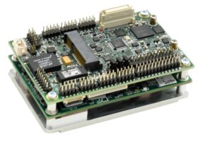
Embedded PCB Example
A printed circuit board (PCB) mechanically supports and electrically connects electronic components using conductive tracks, pads and other features etched from copper sheets laminated onto a non-conductive substrate. Advanced PCB’s may contain components – capacitors, resistors or active devices – embedded in the substrate.
Printed circuit boards are used in all but the simplest electronic products. Alternatives to PCBs include wire wrap and point-to-point construction. PCBs are more costly to design but allow automated manufacturing and assembly. Products are then faster and cheaper to manufacture, and potentially more reliable.
The general progression for a commercial printed circuit board design would include:[2]
- Schematic capture through an electronic design automation tool.
- Card dimensions and template are decided based on required circuitry and case of the PCB. Determine the fixed components and heat sinks if required.
- Deciding stack layers of the PCB. 1 to 12 layers or more depending on design complexity. Ground plane and power plane are decided. Signal planes where signals are routed are in top layer as well as internal layers.
- Line impedance determination using dielectric layer thickness, routing copper thickness and trace-width. Trace separation also taken into account in case of differential signals.
- Placement of the components. Thermal considerations and geometry are taken into account. Vias and lands are marked.
- Routing the signal traces. For optimal EMI performance high frequency signals are routed in internal layers between power or ground planes as power planes behave as ground for AC.
- Gerber file generation for manufacturing.
After the printed circuit board (PCB) is completed, electronic components must be attached to form a functional printed circuit assembly, or PCA (sometimes called a “printed circuit board assembly” PCBA). In through-hole construction, component leads are inserted in holes. In surface-mount construction, the components are placed on pads or lands on the outer surfaces of the PCB. In both kinds of construction, component leads are electrically and mechanically fixed to the board with a molten metal solder.
There are a variety of soldering techniques used to attach components to a PCB. High volume production is usually done with SMT placement machine and bulk wave soldering or reflow ovens, but skilled technicians are able to solder very tiny parts (for instance 0201 packages which are 0.02 in. by 0.01 in.) by hand under a microscope, using tweezers and a fine tip soldering iron for small volume prototypes. Some parts may be extremely difficult to solder by hand, such as BGA packages.
After the board has been populated it may be tested in a variety of ways:
- While the power is off, visual inspection, automated optical inspection. IDEC guidelines for PCB component placement, soldering, and inspection are commonly used to maintain quality control in this stage of PCB manufacturing.
- While the power is off, analog signature analysis, power-off testing.
- While the power is on, in-circuit test, where physical measurements (for example, voltage) can be done.
- While the power is on, functional test, checking if the PCB does what it had been designed to do.
In boundary scan testing, test circuits integrated into various ICs on the board form temporary connections between the PCB traces to test that the ICs are mounted correctly. Boundary scan testing requires that all the ICs to be tested use a standard test configuration procedure, the most common one being the Joint Test Action Group standard. The ITAG test architecture provides a means to test interconnects between integrated circuits on a board without using physical test probes. ITAG tool vendors provide various types of stimulus and sophisticated algorithms, not only to detect the failing nets, but also to isolate the faults to specific nets, devices, and pins.
When boards fail the test, technicians may de-solder and replace failed components, a task known as rework.
Contact EMCOT at: 713-937-4553 S.Spaw@emcotcorp.com